Explore the offer

Advanced Characterization and Fine Analysis / Scanning probe microscopy

Atomic Force Microscopy

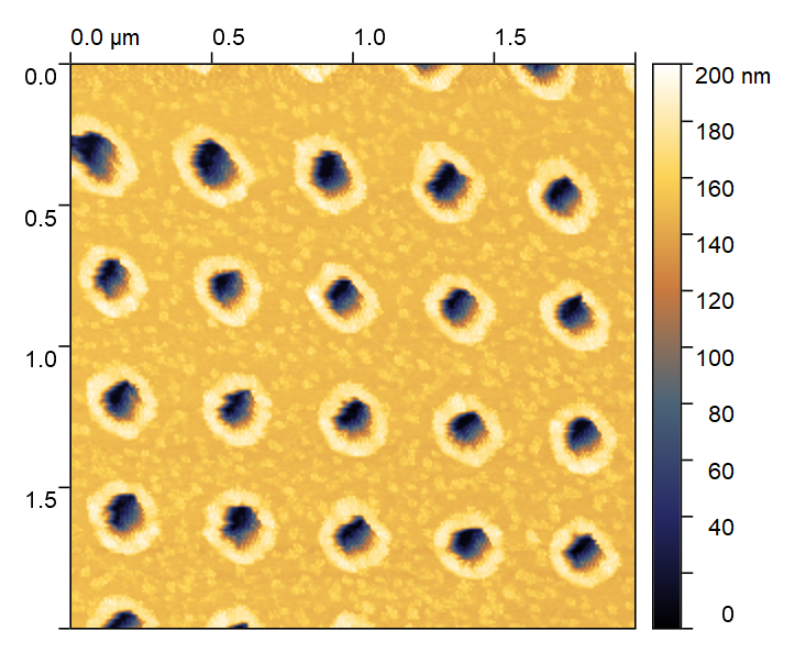
AFM is a surface sensitive technique permitting to obtain a microscopic image of the topography of a material surface. Typical lateral image sizes are within a range of only a few Nanometers to several 10 Micrometers, whereas height changes of less than a Nanometer may be resolved.

A fine tip attached to a cantilever is scanned across the material surface and enables to measure height changes exploiting an optical beam deflection system (a laser that is reflected from the rear side of the cantilever onto a segmented photodiode). The position of a laser spot on the photodiode permits to track height changes as e.g. due to a nano-particle on the surface or an atomic terrace of a single crystal surface. A feedback loop controls the tip-surface distance and therefore ensures stable imaging conditions.

Different operation modes like contact or non-contact mode can be used to optimize the imaging conditions with highest lateral resolution on one hand and least sample interaction on the other hand. Measurements in different environmental conditions (liquid, gas,...) on a broad class of samples (smooth, rough, insulating, conductive, soft, stiff, wet, dry...) can be performed.

Choosing suitable tips and imaging modes, additional surface properties can be mapped together with the topography, with similar spatial resolution, like friction force, magnetization and surface potential, surface charge density and electrical resistance, as well as elastic modulus and adhesion of heterogeneous sample surfaces can be obtained. 

Available instruments

Select instruments to view their specifications and compare them (3 max)

Lab's Facility

Milano

POLIMI-POLIFAB

Milano

UNIMI-Fisica

Instruments' description and comparison

Also consider

In a scanning electron microscope (SEM), an electron beam is scanned over the sample surface in a raster pattern while signals from secondary electrons (SE) or Back-scattered electrons (BSE) are recorded by specific electron detectors. The electron beam, typically with an energy ranging from a few hundred eV up to 30 keV, is focused to a spot of about 0.4 nm to 5 nm in diameter. The latest generation of SEMs can achieve a resolution of 0.4 nm at 30 kV and 0.9 nm at 1 kV.

Beyond the ability to image a comparatively large area of the specimen, SEM can be equipped with a variety of analytical techniques for measuring the specimen's composition. Chemical composition analysis can be performed by Energy Dispersive X-ray Spectroscopy (EDS), which relies on generating an X-ray spectrum from the entire scan area of the SEM. An EDS detector mounted in the SEM chamber collects and separates the characteristic X-rays of different elements into an energy spectrum. The EDS system software then analyzes this energy spectrum to determine the abundance of specific elements. EDS can identify the chemical composition of materials down to a spot size and create elemental composition maps over a much broader raster area.

By employing a suitable polarimeter, such as a Mott analyzer, the spin polarization of secondary electrons can be detected, thus revealing the magnetization orientation in a ferromagnetic sample with high spatial resolution. This technique is known as Scanning Electron Microscopy with Polarization Analysis (SEMPA).

Scanning transmission electron microscopy (STEM) can be also performed in a SEM. It provides high-resolution images and detailed information about the composition and structure of samples, making it an essential tool in various scientific fields. STEM Images can be of different types: Bright-Field (BF) images formed by transmitted electrons that pass through the sample without significant scattering; Annular Dark-Field (ADF) images formed by high-angle scattered electrons, providing information about the atomic number distribution in the sample, and; High-Angle Annular Dark-Field (HAADF) images formed by very high-angle scattered electrons, revealing the heaviest elements in the sample with high contrast.

Read more

SEM

Scanning Electron Microscopy

Advanced Characterization and Fine Analysis

Ultrafast spectroscopy (or Pump-probe spectroscopy) is a technique used to study the dynamics of excited states in various materials, such as molecules, semiconductors, and solids.

It involves the use of two laser pulses. The first laser pulse, the "pump," excites the sample, elevating electrons from the ground state to an excited state. This initiation creates a non-equilibrium condition in the sample. After a controlled delay, a second laser pulse, the "probe," is sent through the sample. The probe pulse interrogates the sample to gather information about the transient states and the evolution of the excited states over time.

By varying the delay time between the pump and probe pulses, researchers can create a time-resolved picture of the dynamic processes occurring in the material. This time resolution can be on the order of femtoseconds (10^-15 seconds), allowing scientists to observe ultrafast phenomena.

These techniques provide insights into ultrafast processes, such as electronic transitions, high-order harmonics generation, molecular vibrations, and energy transfer mechanisms, that occur on very short time scales. It helps in understanding the fundamental properties of materials, such as the relaxation times of excited states, carrier dynamics in semiconductors, topological effects and the mechanisms of photochemical reactions.

Other possible studies can cover the world of solar cells, light-emitting devices, and photocatalysts, where understanding the dynamics of excited states is essential for improving efficiency and performance. Moreover, in biophysics and biochemistry, pump-probe spectroscopy can be used to investigate the dynamics of biomolecules, such as the folding and unfolding of proteins, photosynthesis mechanisms, and the behavior of molecular motors.

Read more

US

Ultrafast-Spectroscopy

Advanced Characterization and Fine Analysis

Latest publications on the subject

View all