Explore the offer

Upscale to Intermediate TRL / Micro-fabrication and Large Area Deposition

Large Area Direct write lithography

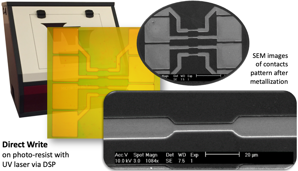
In front of or additionally to traditional photolithography, where the use of a photomask and a mask aligner tool or a reticle and a stepper are needed to transfer the designed layouts onto the substrates via a photosensitive resist coating, Direct Writing Lithography constitutes another photolithography technique which provides a fast and versatile technology especially suited for its use in R+D or in the prototyping stages.

In this technology, Direct laser writers are used in nsubstitution of traditional mask aligners or even steppers to directly expose the photoresist that is covering the surface of the substrates, being controlled by a software which reads the patterns in the designed layout (for instance GDS files) and guides a deflector to reproduce the patterns onto the resist.

Some tools can combine two approaches of photoresist exposition: the rasterized approach, for larger patterns, and the vectorial direct writing approach, where the radiation is focused to a narrow beam that is scanned in vector form across the resist, which allows the best resolution at the cost of lowering the exposition speed.

Noticeably, a key advantage of maskless lithography is the ability to change lithography patterns from one run to the next, avoiding incurring in most of the costs of generating a new photomask, both in economical and time terms.

Available instruments

Select instruments to view their specifications and compare them (3 max)

Lab's Facility

Milano

UNIMI-Fisica

Milano

POLIMI-POLIFAB

Instruments' description and comparison

Also consider

AFM is a surface sensitive technique permitting to obtain a microscopic image of the topography of a material surface. Typical lateral image sizes are within a range of only a few Nanometers to several 10 Micrometers, whereas height changes of less than a Nanometer may be resolved.

A fine tip attached to a cantilever is scanned across the material surface and enables to measure height changes exploiting an optical beam deflection system (a laser that is reflected from the rear side of the cantilever onto a segmented photodiode). The position of a laser spot on the photodiode permits to track height changes as e.g. due to a nano-particle on the surface or an atomic terrace of a single crystal surface. A feedback loop controls the tip-surface distance and therefore ensures stable imaging conditions.

Different operation modes like contact or non-contact mode can be used to optimize the imaging conditions with highest lateral resolution on one hand and least sample interaction on the other hand. Measurements in different environmental conditions (liquid, gas,...) on a broad class of samples (smooth, rough, insulating, conductive, soft, stiff, wet, dry...) can be performed.

Choosing suitable tips and imaging modes, additional surface properties can be mapped together with the topography, with similar spatial resolution, like friction force, magnetization and surface potential, surface charge density and electrical resistance, as well as elastic modulus and adhesion of heterogeneous sample surfaces can be obtained. 

Read more

AFM

Atomic Force Microscopy

Advanced Characterization and Fine Analysis