Explore the offer
Upscale to Intermediate TRL / Micro-fabrication
Dicing-saw
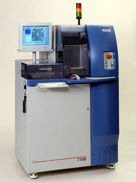
Dicing is typically used to separate die from a wafer to be mounted in a package or on a PC board. Some users dice a wafer into smaller pieces to process individually. It can be used to cut a wide range of materials and devices including Semiconductor devices, Ceramic Substrates, Thick-film Devices, Sensors, MEMS, Opto-electronic Components, IC Wafers.
Some tools are optimized for multi-angle dicing of thin, tight tolerance products up to 150 mm or 6" diameter and capable of more complex patterns such as multiple indexes and varying cut depths.
Wafers are typically mounted on dicing tape which has an adhesive backing that holds the wafer on a metal frame. The frame with the wafer on it is placed on the chuck of the dicing saw. The wafer is moved into an abrasive blade, usually diamond, rotating at typically 15,000 to 30,000 RPM. The abrasive chips away at the wafer as the blade rotates. Water is supplied to the blade to remove cutting residue and enhance cut quality.
The cut depth is a function of the substrate thickness and could be optimized depending on the cut quality and blade loading. A good rule of thumb is to cut no more than about 500 µm of material per pass. Harder materials should be cut with shallower cuts and more passes to minimize blade wear. Deeper cuts require a thicker blade to minimize blade flexing or deflection.
Available instruments
Select instruments to view their specifications and compare them (3 max)
Lab's Facility
Bologna
CNR-ISMN@BO
Milano