Explore the offer

Growth & Synthesis / Chemical depositions of thin films

Atomic Layer Deposition

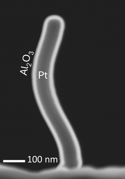
Atomic Layer Deposition (ALD) is similar to CVD except that the ALD reaction occurs at lower temperature and it is broken into two half-reactions, keeping the precursor materials separated during the reaction. The separation of the precursors is important to achieve a self-limiting surface reaction to enable precise thickness control and ensure uniform coatings and compactness even in complicated 3D structures.

The present implementation of the technique is suitable for mm to cm-size samples as those typically studied by spectroscopy and microscopy.

ALD has a rich history in microelectronics. It is studied as a potential technique to deposit high-k (high permittivity) gate oxides, high-k memory capacitor dielectrics, ferroelectrics, and metals and nitrides for electrodes and interconnects.

The number of materials that can be prepared by ALD has tremendously increased in the past decade. Notably, it can deposit a wider variety of materials, including important functional oxides like Al2O3, MoO3, SiO2 and HfO2.

Available instruments

Select instruments to view their specifications and compare them (3 max)

Lab's Facility

Lecce

CNR-NANOTEC@LE

Milano

POLIMI-POLIFAB

Instruments' description and comparison

Also consider

In a scanning electron microscope (SEM), an electron beam is scanned over the sample surface in a raster pattern while signals from secondary electrons (SE) or Back-scattered electrons (BSE) are recorded by specific electron detectors. The electron beam, typically with an energy ranging from a few hundred eV up to 30 keV, is focused to a spot of about 0.4 nm to 5 nm in diameter. The latest generation of SEMs can achieve a resolution of 0.4 nm at 30 kV and 0.9 nm at 1 kV.

Beyond the ability to image a comparatively large area of the specimen, SEM can be equipped with a variety of analytical techniques for measuring the specimen's composition. Chemical composition analysis can be performed by Energy Dispersive X-ray Spectroscopy (EDS), which relies on generating an X-ray spectrum from the entire scan area of the SEM. An EDS detector mounted in the SEM chamber collects and separates the characteristic X-rays of different elements into an energy spectrum. The EDS system software then analyzes this energy spectrum to determine the abundance of specific elements. EDS can identify the chemical composition of materials down to a spot size and create elemental composition maps over a much broader raster area.

By employing a suitable polarimeter, such as a Mott analyzer, the spin polarization of secondary electrons can be detected, thus revealing the magnetization orientation in a ferromagnetic sample with high spatial resolution. This technique is known as Scanning Electron Microscopy with Polarization Analysis (SEMPA).

Scanning transmission electron microscopy (STEM) can be also performed in a SEM. It provides high-resolution images and detailed information about the composition and structure of samples, making it an essential tool in various scientific fields. STEM Images can be of different types: Bright-Field (BF) images formed by transmitted electrons that pass through the sample without significant scattering; Annular Dark-Field (ADF) images formed by high-angle scattered electrons, providing information about the atomic number distribution in the sample, and; High-Angle Annular Dark-Field (HAADF) images formed by very high-angle scattered electrons, revealing the heaviest elements in the sample with high contrast.

Read more

SEM

Scanning Electron Microscopy

Advanced Characterization and Fine Analysis

AFM is a surface sensitive technique permitting to obtain a microscopic image of the topography of a material surface. Typical lateral image sizes are within a range of only a few Nanometers to several 10 Micrometers, whereas height changes of less than a Nanometer may be resolved.

A fine tip attached to a cantilever is scanned across the material surface and enables to measure height changes exploiting an optical beam deflection system (a laser that is reflected from the rear side of the cantilever onto a segmented photodiode). The position of a laser spot on the photodiode permits to track height changes as e.g. due to a nano-particle on the surface or an atomic terrace of a single crystal surface. A feedback loop controls the tip-surface distance and therefore ensures stable imaging conditions.

Different operation modes like contact or non-contact mode can be used to optimize the imaging conditions with highest lateral resolution on one hand and least sample interaction on the other hand. Measurements in different environmental conditions (liquid, gas,...) on a broad class of samples (smooth, rough, insulating, conductive, soft, stiff, wet, dry...) can be performed.

Choosing suitable tips and imaging modes, additional surface properties can be mapped together with the topography, with similar spatial resolution, like friction force, magnetization and surface potential, surface charge density and electrical resistance, as well as elastic modulus and adhesion of heterogeneous sample surfaces can be obtained. 

Read more

AFM

Atomic Force Microscopy

Advanced Characterization and Fine Analysis