Explore the offer
Advanced Characterization and Fine Analysis / Electron, Ion and photon beam microscopy
Scanning Electron Microscopy
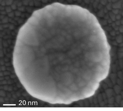
In a scanning electron microscope (SEM), an electron beam is scanned over the sample surface in a raster pattern while signals from secondary electrons (SE) or Back-scattered electrons (BSE) are recorded by specific electron detectors. The electron beam, typically with an energy ranging from a few hundred eV up to 30 keV, is focused to a spot of about 0.4 nm to 5 nm in diameter. The latest generation of SEMs can achieve a resolution of 0.4 nm at 30 kV and 0.9 nm at 1 kV.
Beyond the ability to image a comparatively large area of the specimen, SEM can be equipped with a variety of analytical techniques for measuring the specimen's composition. Chemical composition analysis can be performed by Energy Dispersive X-ray Spectroscopy (EDS), which relies on generating an X-ray spectrum from the entire scan area of the SEM. An EDS detector mounted in the SEM chamber collects and separates the characteristic X-rays of different elements into an energy spectrum. The EDS system software then analyzes this energy spectrum to determine the abundance of specific elements. EDS can identify the chemical composition of materials down to a spot size and create elemental composition maps over a much broader raster area.
By employing a suitable polarimeter, such as a Mott analyzer, the spin polarization of secondary electrons can be detected, thus revealing the magnetization orientation in a ferromagnetic sample with high spatial resolution. This technique is known as Scanning Electron Microscopy with Polarization Analysis (SEMPA).
Scanning transmission electron microscopy (STEM) can be also performed in a SEM. It provides high-resolution images and detailed information about the composition and structure of samples, making it an essential tool in various scientific fields. STEM Images can be of different types: Bright-Field (BF) images formed by transmitted electrons that pass through the sample without significant scattering; Annular Dark-Field (ADF) images formed by high-angle scattered electrons, providing information about the atomic number distribution in the sample, and; High-Angle Annular Dark-Field (HAADF) images formed by very high-angle scattered electrons, revealing the heaviest elements in the sample with high contrast.
Available instruments
Select instruments to view their specifications and compare them (3 max)
Lab's Facility
Catania
CNR-IMM@CT
Lecce
CNR-NANOTEC@LE
Milano
POLIMI-POLIFAB
Trento