Explore the offer

Growth & Synthesis / Physical depositions of thin films

Pulsed Laser Deposition

PLD is a physical vapor deposition technique in which the pulsed beam of a high-power ultraviolet laser is focused inside a vacuum chamber on a target. The target is usually a sintered ceramic or a single crystal with the chemical composition of the film that is to be deposited. A significant removal of material occurs above a certain threshold energy density (depending on the material, laser wavelength and pulse duration). The ejected material forms a luminous ablation plume directed towards a substrate placed front the target at a distance of 4-8 cm, where it re-condenses to form a film. Usually the plume (composed by neutrals, ions and electrons, and more complex species) conserves the stoichiometry of the target. The deposition can occur either in ultra-high-vacuum as well as in a background gas (up to 1 mbar) such as oxygen, which is commonly used when depositing oxides.

A main characteristic of PLD is that the ablated material only arrives at the substrate during a few microseconds after each the nanosecond laser pulse. It is also relevant that atoms and ions in the plume have an energy that can be controlled by the pressure during deposition and other parameters. PLD is compatible with in-situ and-real-time characterization tools, like reflection high-energy electron diffraction. A limitation of PLD is the small deposition area, generally less than 1 cm2 in standard set-ups (although a system for large area PLD up to 4 inches is available in the consortium). Another limitation is that the plume is highly directional, and thus not suitable for conformal deposition of non-flat substrates.

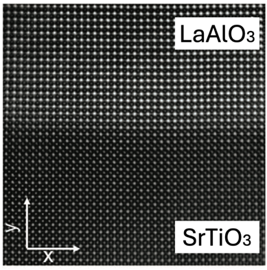
PLD has been used to deposit films of a variety of materials. It is extensively used to produce copper oxide superconductors, ferroelectric and ferromagnetic oxides, etc. Its use is not limited to grow complex oxides, but can be extended to other materials, including diamond-like carbon, refractory materials, 2D materials and even metals.

Available instruments

Select instruments to view their specifications and compare them (3 max)

Lab's Facility

Napoli

CNR-SPIN@NA

Milano

POLIMI-POLIFAB

Trieste

CNR-IOM@TS

Instruments' description and comparison

Also consider

In a scanning electron microscope (SEM), an electron beam is scanned over the sample surface in a raster pattern while signals from secondary electrons (SE) or Back-scattered electrons (BSE) are recorded by specific electron detectors. The electron beam, typically with an energy ranging from a few hundred eV up to 30 keV, is focused to a spot of about 0.4 nm to 5 nm in diameter. The latest generation of SEMs can achieve a resolution of 0.4 nm at 30 kV and 0.9 nm at 1 kV.

Beyond the ability to image a comparatively large area of the specimen, SEM can be equipped with a variety of analytical techniques for measuring the specimen's composition. Chemical composition analysis can be performed by Energy Dispersive X-ray Spectroscopy (EDS), which relies on generating an X-ray spectrum from the entire scan area of the SEM. An EDS detector mounted in the SEM chamber collects and separates the characteristic X-rays of different elements into an energy spectrum. The EDS system software then analyzes this energy spectrum to determine the abundance of specific elements. EDS can identify the chemical composition of materials down to a spot size and create elemental composition maps over a much broader raster area.

By employing a suitable polarimeter, such as a Mott analyzer, the spin polarization of secondary electrons can be detected, thus revealing the magnetization orientation in a ferromagnetic sample with high spatial resolution. This technique is known as Scanning Electron Microscopy with Polarization Analysis (SEMPA).

Scanning transmission electron microscopy (STEM) can be also performed in a SEM. It provides high-resolution images and detailed information about the composition and structure of samples, making it an essential tool in various scientific fields. STEM Images can be of different types: Bright-Field (BF) images formed by transmitted electrons that pass through the sample without significant scattering; Annular Dark-Field (ADF) images formed by high-angle scattered electrons, providing information about the atomic number distribution in the sample, and; High-Angle Annular Dark-Field (HAADF) images formed by very high-angle scattered electrons, revealing the heaviest elements in the sample with high contrast.

Read more

SEM

Scanning Electron Microscopy

Advanced Characterization and Fine Analysis

AFM is a surface sensitive technique permitting to obtain a microscopic image of the topography of a material surface. Typical lateral image sizes are within a range of only a few Nanometers to several 10 Micrometers, whereas height changes of less than a Nanometer may be resolved.

A fine tip attached to a cantilever is scanned across the material surface and enables to measure height changes exploiting an optical beam deflection system (a laser that is reflected from the rear side of the cantilever onto a segmented photodiode). The position of a laser spot on the photodiode permits to track height changes as e.g. due to a nano-particle on the surface or an atomic terrace of a single crystal surface. A feedback loop controls the tip-surface distance and therefore ensures stable imaging conditions.

Different operation modes like contact or non-contact mode can be used to optimize the imaging conditions with highest lateral resolution on one hand and least sample interaction on the other hand. Measurements in different environmental conditions (liquid, gas,...) on a broad class of samples (smooth, rough, insulating, conductive, soft, stiff, wet, dry...) can be performed.

Choosing suitable tips and imaging modes, additional surface properties can be mapped together with the topography, with similar spatial resolution, like friction force, magnetization and surface potential, surface charge density and electrical resistance, as well as elastic modulus and adhesion of heterogeneous sample surfaces can be obtained. 

Read more

AFM

Atomic Force Microscopy

Advanced Characterization and Fine Analysis

Transmission Electron Microscopes (TEM) and Scanning Transmission Electron Microscopes (STEM)  are designed for high-resolution imaging and analysis.
In both cases, high energy electrons, incident on ultra-thin samples called TEM lamella (typically <100nm), travel through the specimen.
Depending on the density, crystallinity, orientation, etc. of the material present, electrons are scattered differently, giving rise to an image of the sample with different contrast features according to specimen properties and to the microscope setup.
Usually, the magnified image of the sample is focused on a CCD or CMOS camera. On the same system is also possible to acquire the electron diffraction produced by a specific area of the sample.

Modern TEM are equipped with a Cold Field Emission Gun (FEG) or with a Schottky FEG, making them suitable for materials science, nanotechnology, and various fields requiring detailed structural and compositional analysis in a local nanoscale. Indeed, point resolution below 0.3 nm at 200kV in TEM mode can be reached, according to the
instrument configuration.


In the STEM mode, electrons pass through the specimen, but, the electron optics focus the beam into a narrow spot which is scanned over the sample in a raster. The rastering of the beam across the sample makes these microscopes suitable for analysis techniques.


According to the specific configuration (see details and the specific availability below, referred to each instrument and facility), the microscope can be equipped with a selection of multiple detectors enabling different techniques, such as Energy-Dispersive x-ray Spectroscopy analysis (EDS), electron energy loss spectroscopy (EELS), STEM detectors in bright field (BF), annular bright field (ABF), annular dark field (ADF) for diffraction contrast, high-angle annular dark field (HAADF) for Z-contrast.


EELS/EDS system control software enables point-by-point signal acquisitions, for the analysis of spectra and maps.
Sample preparation (see details and the specific availability below, referred to each instrument and facility) is a crucial part in TEM experiments.

High quality TEM specimens have a thickness that is comparable to the mean free path of the electrons that travel through the samples, which may be only a few tens of nanometres. Preparation of TEM specimens is specific to the material under analysis and the desired information to obtain from the specimen. Sample preparation laboratories are equipped with the basic tools (diamond saw, polisher, dimpler, ultrasonic cutter, precision ion polishing system, plasma cleaner) commonly used in conventional thinning procedures.

Read more

TEM/STEM

Transmission Electron Microscopes and Scanning Transmission Electron Microscopes

Advanced Characterization and Fine Analysis

The facility consists of a magneto-transport equipment for electrical characterization integrated in a cryogen-free measurement system at variable temperature and magnetic fields. It has capabilities for 2-point or 4-point measurements, for Hall effect measurements in the Van der Pauw and Hall bar geometries, as well as I-V and C-V characteristics in DC and AC modes. This allows study of electrical transport (both semiclassical, i.e. conductivity and electric carrier density and mobility, and quantum transport effects in nano- and mesoscopic devices) on material systems such as semiconductor low-D structures (2DEGs, nanowires…), 2D and 1D materials (graphene and graphene-like nanomaterials, nanotubes, transition metal dichalcogenides, ultrathin 2D-oxides…), topological insulators and superconductors.  Additional electrical contacts allow application of gate biases for sample polarization. Electric Transport-Optical measurements in Electro-Optical and Magneto-optical configurations are possible through a tuneable Xenon light source and fibre-optic sample illumination.

Samples are fitted in a 16-pin dual-in-line socket, which can be placed perpendicular or parallel to the magnetic field. All 16 electrical connections can be independently and automatically switched through a matrix switch unit under software control. Samples with a wide range of resistivities can be measured, ranging from diluted 2D electron gases in semiconductors to metals. It is possible to record sweeps of gate voltages and magnetic fields (for, e.g., the observation of Shubnikov–de Haas oscillations / Quantum Hall effect in semiconductor 2D systems), as well as of temperature.

Read more

MT

Magneto-Transport

Advanced Characterization and Fine Analysis