Explore the offer

Advanced Characterization and Fine Analysis / Magnetic characterisation

Magneto-Transport

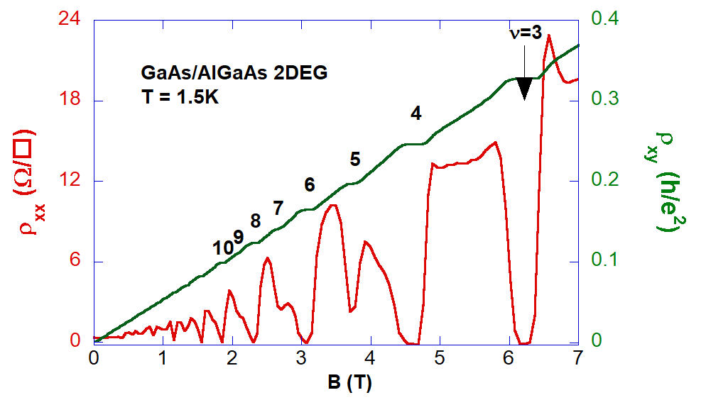
The facility consists of a magneto-transport equipment for electrical characterization integrated in a cryogen-free measurement system at variable temperature and magnetic fields. It has capabilities for 2-point or 4-point measurements, for Hall effect measurements in the Van der Pauw and Hall bar geometries, as well as I-V and C-V characteristics in DC and AC modes. This allows study of electrical transport (both semiclassical, i.e. conductivity and electric carrier density and mobility, and quantum transport effects in nano- and mesoscopic devices) on material systems such as semiconductor low-D structures (2DEGs, nanowires…), 2D and 1D materials (graphene and graphene-like nanomaterials, nanotubes, transition metal dichalcogenides, ultrathin 2D-oxides…), topological insulators and superconductors.  Additional electrical contacts allow application of gate biases for sample polarization. Electric Transport-Optical measurements in Electro-Optical and Magneto-optical configurations are possible through a tuneable Xenon light source and fibre-optic sample illumination.

Samples are fitted in a 16-pin dual-in-line socket, which can be placed perpendicular or parallel to the magnetic field. All 16 electrical connections can be independently and automatically switched through a matrix switch unit under software control. Samples with a wide range of resistivities can be measured, ranging from diluted 2D electron gases in semiconductors to metals. It is possible to record sweeps of gate voltages and magnetic fields (for, e.g., the observation of Shubnikov–de Haas oscillations / Quantum Hall effect in semiconductor 2D systems), as well as of temperature.

Available instruments

Select instruments to view their specifications and compare them (3 max)

Lab's Facility

Trieste

CNR-IOM@TS

Instruments' description and comparison

Also consider

In a scanning electron microscope (SEM), an electron beam is scanned over the sample surface in a raster pattern while signals from secondary electrons (SE) or Back-scattered electrons (BSE) are recorded by specific electron detectors. The electron beam, typically with an energy ranging from a few hundred eV up to 30 keV, is focused to a spot of about 0.4 nm to 5 nm in diameter. The latest generation of SEMs can achieve a resolution of 0.4 nm at 30 kV and 0.9 nm at 1 kV.

Beyond the ability to image a comparatively large area of the specimen, SEM can be equipped with a variety of analytical techniques for measuring the specimen's composition. Chemical composition analysis can be performed by Energy Dispersive X-ray Spectroscopy (EDS), which relies on generating an X-ray spectrum from the entire scan area of the SEM. An EDS detector mounted in the SEM chamber collects and separates the characteristic X-rays of different elements into an energy spectrum. The EDS system software then analyzes this energy spectrum to determine the abundance of specific elements. EDS can identify the chemical composition of materials down to a spot size and create elemental composition maps over a much broader raster area.

By employing a suitable polarimeter, such as a Mott analyzer, the spin polarization of secondary electrons can be detected, thus revealing the magnetization orientation in a ferromagnetic sample with high spatial resolution. This technique is known as Scanning Electron Microscopy with Polarization Analysis (SEMPA).

Scanning transmission electron microscopy (STEM) can be also performed in a SEM. It provides high-resolution images and detailed information about the composition and structure of samples, making it an essential tool in various scientific fields. STEM Images can be of different types: Bright-Field (BF) images formed by transmitted electrons that pass through the sample without significant scattering; Annular Dark-Field (ADF) images formed by high-angle scattered electrons, providing information about the atomic number distribution in the sample, and; High-Angle Annular Dark-Field (HAADF) images formed by very high-angle scattered electrons, revealing the heaviest elements in the sample with high contrast.

Read more

SEM

Scanning Electron Microscopy

Advanced Characterization and Fine Analysis

PLD is a physical vapor deposition technique in which the pulsed beam of a high-power ultraviolet laser is focused inside a vacuum chamber on a target. The target is usually a sintered ceramic or a single crystal with the chemical composition of the film that is to be deposited. A significant removal of material occurs above a certain threshold energy density (depending on the material, laser wavelength and pulse duration). The ejected material forms a luminous ablation plume directed towards a substrate placed front the target at a distance of 4-8 cm, where it re-condenses to form a film. Usually the plume (composed by neutrals, ions and electrons, and more complex species) conserves the stoichiometry of the target. The deposition can occur either in ultra-high-vacuum as well as in a background gas (up to 1 mbar) such as oxygen, which is commonly used when depositing oxides.

A main characteristic of PLD is that the ablated material only arrives at the substrate during a few microseconds after each the nanosecond laser pulse. It is also relevant that atoms and ions in the plume have an energy that can be controlled by the pressure during deposition and other parameters. PLD is compatible with in-situ and-real-time characterization tools, like reflection high-energy electron diffraction. A limitation of PLD is the small deposition area, generally less than 1 cm2 in standard set-ups (although a system for large area PLD up to 4 inches is available in the consortium). Another limitation is that the plume is highly directional, and thus not suitable for conformal deposition of non-flat substrates.

PLD has been used to deposit films of a variety of materials. It is extensively used to produce copper oxide superconductors, ferroelectric and ferromagnetic oxides, etc. Its use is not limited to grow complex oxides, but can be extended to other materials, including diamond-like carbon, refractory materials, 2D materials and even metals.

Read more

PLD

Pulsed Laser Deposition

Growth & Synthesis