Explore the offer

Upscale to Intermediate TRL / OPTO-ELECTRONIC CHARACTERIZATION

Charge Extraction by Linearly Increasing Voltage

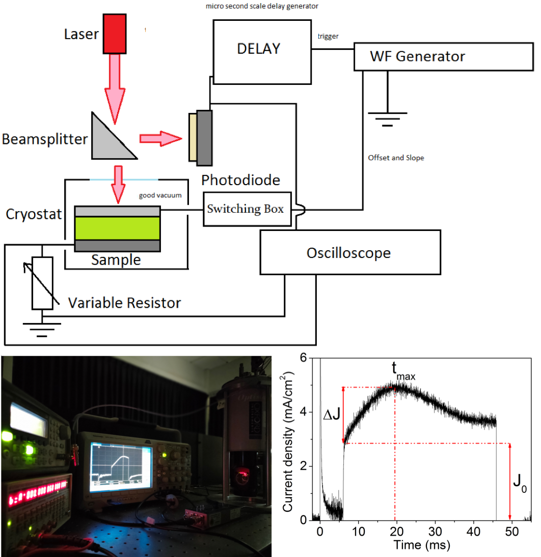
Charge Extraction by Linearly Increasing Voltage (CELIV) is a popular technique usually used to estimate charge carrier mobilities in organic and perovskite based optoelectronic devices. A displacement current generated within the active layer by an external trigger can be recorded and used to extract significant information about the material itself, such as mobility, doping, relative permittivity, recombination coefficient.

We can perform various modifications of the CELIV technique: Dark-CELIV, Photo-CELIV, Injection-CELIV, and MIS-CELIV. The set-up is flexible enough to convert to CELIV from Time-of-Flight (TOF) measurements (and vice versa) very rapidly so that it can be used for many different optoelectronic devices with minimal alterations. Figure on the right shows a schematic of the CELIV set-up used.

Measurements can be performed under different environmental conditions, such as in air, under inert atmosphere (N2) or in vacuum, by placing the device inside a customized cryostat in a sample holder which supplied signal to the contacts and gave light access to the device for photo-excitation. The light source is a pulsed LASER tunable over the UV, VIS and NIR spectrum to give the appropriate excitation to a wide range of materials. Finally, measurements can be performed in a temperature range varying from 77 K up to 400 K.

Available instruments

Select instruments to view their specifications and compare them (3 max)

Lab's Facility

Lecce

CNR-NANOTEC@LE

Instruments' description and comparison

Also consider

The facility consists of a magneto-transport equipment for electrical characterization integrated in a cryogen-free measurement system at variable temperature and magnetic fields. It has capabilities for 2-point or 4-point measurements, for Hall effect measurements in the Van der Pauw and Hall bar geometries, as well as I-V and C-V characteristics in DC and AC modes. This allows study of electrical transport (both semiclassical, i.e. conductivity and electric carrier density and mobility, and quantum transport effects in nano- and mesoscopic devices) on material systems such as semiconductor low-D structures (2DEGs, nanowires…), 2D and 1D materials (graphene and graphene-like nanomaterials, nanotubes, transition metal dichalcogenides, ultrathin 2D-oxides…), topological insulators and superconductors.  Additional electrical contacts allow application of gate biases for sample polarization. Electric Transport-Optical measurements in Electro-Optical and Magneto-optical configurations are possible through a tuneable Xenon light source and fibre-optic sample illumination.

Samples are fitted in a 16-pin dual-in-line socket, which can be placed perpendicular or parallel to the magnetic field. All 16 electrical connections can be independently and automatically switched through a matrix switch unit under software control. Samples with a wide range of resistivities can be measured, ranging from diluted 2D electron gases in semiconductors to metals. It is possible to record sweeps of gate voltages and magnetic fields (for, e.g., the observation of Shubnikov–de Haas oscillations / Quantum Hall effect in semiconductor 2D systems), as well as of temperature.

Read more

MT

Magneto-Transport

Advanced Characterization and Fine Analysis