Explore the offer

Advanced Characterization and Fine Analysis / Electron spectroscopy

Photo-Electron Spectroscopy

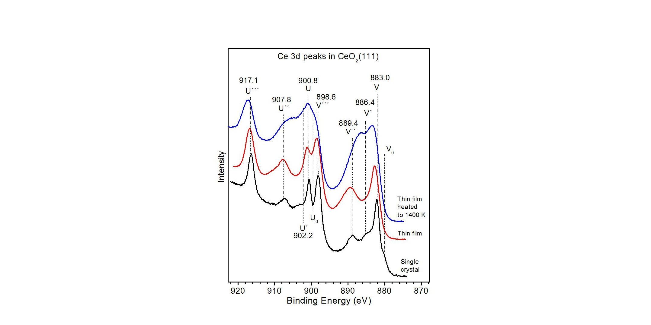
PES (Photo-electron Spectroscopy) is a general term that includes X-ray Photoelectron Spectroscopy (XPS), also known as Electron Spectroscopy for Chemical Analysis (ESCA),  and Ultraviolet Photoelectron Spectroscopy (UPS), that are the most used techniques for the investigation of the chemical properties of the material. In PES, a monochromatic photon beam impinges on the sample and extracts photoelectrons. These photoelectrons are then collected by an electrostatic lens system; their energy dispersion is then measured by an electron energy analyzer. The collected data form the so-called electron dispersion curve (EDC) or photoemission spectrum. From the analysis of the photoemission spectrum, it is possible to derive the chemical composition (stoichiometry) of the material under study and several information about the chemical state of each element, such as oxidation state, chemical bonds, etc. PES can be exploited as a surface chemical analysis technique: the valence band DOS (assessable by UPS) reveals the orbital contributions through cross-section analysis (photon energy dependence) and core level photoemission (assessable by XPS) is sensitive to the local environment of a given atomic species in the first atomic layers of the sample.

Available instruments

Select instruments to view their specifications and compare them (3 max)

Lab's Facility

Trieste

CNR-IOM@TS

Trieste

CNR-IOM@TS

Napoli

CNR-SPIN@NA

Instruments' description and comparison

Also consider

Scanning Tunneling Microscopy (STM) allows imaging conductive surfaces at the atomic scale. It is possible to characterize the distribution of surface terraces and steps, as well as to determine the atomic arrangement of (ordered) surface (over)structures.

In STM, an atomically sharp tip is scanned on a surface at a few-angstrom distance, while a bias voltage is applied between these two electrodes, so that a current flows due to the quantum tunneling effect. The intensity of the tunneling current depends exponentially on the tip-surface distance and can therefore be used to reconstruct a morphologic image.

STM is a local technique: while high-resolution can be achieved on small (nanometer sized) areas, information on large-scale (micron sized or more) is lost, and measurements have to be repeated systematically on several regions of the sample to get statistically relevant information.

Due to stability performances, STM experiments are typically time-consuming. The technique is applicable both in air and in vacuum. Ultra-high-vacuum (UHV) is required for the characterization of delicate, atomically clean systems and for performing measurement at cryogenic temperature.

The STM signal is not purely topographic, but brings also information on the local density of electronic states. Scanning tunneling spectroscopy (STS) is an extension of STM that provides information about the density of electrons in a sample as a function of their energy. Inelastic tunneling spectroscopy (IETS) is a challenging extension for the investigation of vibrational states at liquid helium temperature. The STM tip can also be used to manipulate single atoms and molecules.

By acquiring sequences of consecutive images, STM can also be used to investigate at the atomic scale dynamical processes occurring on the surface of conductive samples, with a typical acquisition time of few tens of seconds per image. To further extend the range of accessible details in this kind of measurements, NFFA-Europe makes for the first time available to external users the access to a FastSTM option for high-speed imaging with a VT-STM microscope at CNR-IOM.  Thanks to this option, it is now possible to image with atomic resolution dynamical processes as chemical reactions, diffusion and growth, with a frame rate up to 100 images per second on regions few-nanometer wide.

Read more

STM

Scanning Tunneling Microscopy

Advanced Characterization and Fine Analysis