Explore the offer

Advanced Characterization and Fine Analysis / Electron, Ion and Photon beam Diffraction

X-Ray Diffraction

XRD is a non-destructive technique used to analyse the structural order of crystalline materials. As a versatile method, XRD provides detailed information about the identity and quantity of crystalline phases present in polymorphic specimens. Additionally, it offers insights into the crystal structure and interplanar distances of the material. This technique can be applied to specimens in various forms, including powders, thin films, and epitaxial films. By measuring the scattering of X-rays at different angles, XRD enables researchers to obtain a comprehensive understanding of the material's crystallography, making it an essential tool in material science and engineering.

The present implementation of the technique is suitable for mm to cm-size samples as those typically studied by spectroscopy and microscopy.

Available instruments

Select instruments to view their specifications and compare them (3 max)

Lab's Facility

Catania

CNR-IMM@CT

Lecce

CNR-NANOTEC@LE

Napoli

CNR-SPIN@NA

Instruments' description and comparison

Also consider

In a scanning electron microscope (SEM), an electron beam is scanned over the sample surface in a raster pattern while signals from secondary electrons (SE) or Back-scattered electrons (BSE) are recorded by specific electron detectors. The electron beam, typically with an energy ranging from a few hundred eV up to 30 keV, is focused to a spot of about 0.4 nm to 5 nm in diameter. The latest generation of SEMs can achieve a resolution of 0.4 nm at 30 kV and 0.9 nm at 1 kV.

Beyond the ability to image a comparatively large area of the specimen, SEM can be equipped with a variety of analytical techniques for measuring the specimen's composition. Chemical composition analysis can be performed by Energy Dispersive X-ray Spectroscopy (EDS), which relies on generating an X-ray spectrum from the entire scan area of the SEM. An EDS detector mounted in the SEM chamber collects and separates the characteristic X-rays of different elements into an energy spectrum. The EDS system software then analyzes this energy spectrum to determine the abundance of specific elements. EDS can identify the chemical composition of materials down to a spot size and create elemental composition maps over a much broader raster area.

By employing a suitable polarimeter, such as a Mott analyzer, the spin polarization of secondary electrons can be detected, thus revealing the magnetization orientation in a ferromagnetic sample with high spatial resolution. This technique is known as Scanning Electron Microscopy with Polarization Analysis (SEMPA).

Scanning transmission electron microscopy (STEM) can be also performed in a SEM. It provides high-resolution images and detailed information about the composition and structure of samples, making it an essential tool in various scientific fields. STEM Images can be of different types: Bright-Field (BF) images formed by transmitted electrons that pass through the sample without significant scattering; Annular Dark-Field (ADF) images formed by high-angle scattered electrons, providing information about the atomic number distribution in the sample, and; High-Angle Annular Dark-Field (HAADF) images formed by very high-angle scattered electrons, revealing the heaviest elements in the sample with high contrast.

Read more

SEM

Scanning Electron Microscopy

Advanced Characterization and Fine Analysis

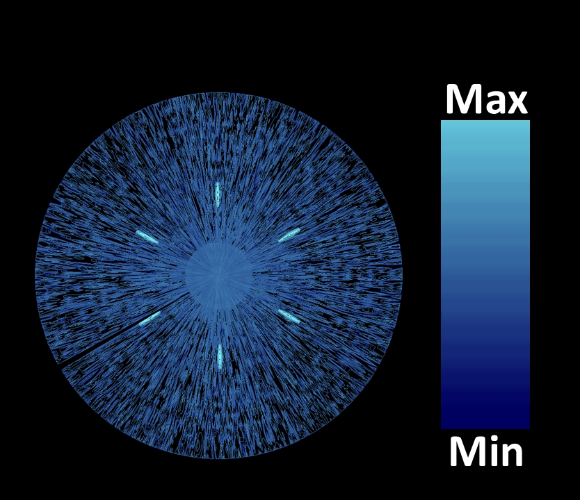
Transmission Electron Microscopes (TEM) and Scanning Transmission Electron Microscopes (STEM)  are designed for high-resolution imaging and analysis.
In both cases, high energy electrons, incident on ultra-thin samples called TEM lamella (typically <100nm), travel through the specimen.
Depending on the density, crystallinity, orientation, etc. of the material present, electrons are scattered differently, giving rise to an image of the sample with different contrast features according to specimen properties and to the microscope setup.
Usually, the magnified image of the sample is focused on a CCD or CMOS camera. On the same system is also possible to acquire the electron diffraction produced by a specific area of the sample.

Modern TEM are equipped with a Cold Field Emission Gun (FEG) or with a Schottky FEG, making them suitable for materials science, nanotechnology, and various fields requiring detailed structural and compositional analysis in a local nanoscale. Indeed, point resolution below 0.3 nm at 200kV in TEM mode can be reached, according to the
instrument configuration.


In the STEM mode, electrons pass through the specimen, but, the electron optics focus the beam into a narrow spot which is scanned over the sample in a raster. The rastering of the beam across the sample makes these microscopes suitable for analysis techniques.


According to the specific configuration (see details and the specific availability below, referred to each instrument and facility), the microscope can be equipped with a selection of multiple detectors enabling different techniques, such as Energy-Dispersive x-ray Spectroscopy analysis (EDS), electron energy loss spectroscopy (EELS), STEM detectors in bright field (BF), annular bright field (ABF), annular dark field (ADF) for diffraction contrast, high-angle annular dark field (HAADF) for Z-contrast.


EELS/EDS system control software enables point-by-point signal acquisitions, for the analysis of spectra and maps.
Sample preparation (see details and the specific availability below, referred to each instrument and facility) is a crucial part in TEM experiments.

High quality TEM specimens have a thickness that is comparable to the mean free path of the electrons that travel through the samples, which may be only a few tens of nanometres. Preparation of TEM specimens is specific to the material under analysis and the desired information to obtain from the specimen. Sample preparation laboratories are equipped with the basic tools (diamond saw, polisher, dimpler, ultrasonic cutter, precision ion polishing system, plasma cleaner) commonly used in conventional thinning procedures.
Read more

TEM/STEM

Transmission Electron Microscopes and Scanning Transmission Electron Microscopes

Advanced Characterization and Fine Analysis