Explore the offer

Upscale to Intermediate TRL / Micro-fabrication and Back-End

Electrochemical deposition

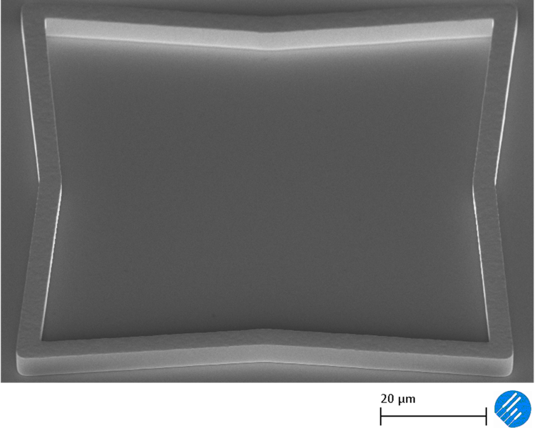
Electrochemical deposition or electroplating is generally used for the deposition of metallic films (Au, Ni) with various advantages. The thickness of the coating can be precisely controlled by adjusting the electrochemical parameters. In addition, compared to standard metal deposition techniques, higher deposition rates can be obtained. The electroplating technique is relatively inexpensive as there are no requirements for high vacuum or high temperature systems.  Moreover the resulting coatings are relatively uniform and compact and standard resists can be used as masks during the electroplating process. Last, electroplating is ideal for relatively thick coatings and structures with high aspect ratios.

Available instruments

Select instruments to view their specifications and compare them (3 max)

Lab's Facility

Milano

POLIMI-POLIFAB

Instruments' description and comparison

Also consider

The Vector Network Analyser is typically used to characterize the electrical response of a system as a function of frequency (from 10 MHz up to 40 GHz). The tool can apply a calibrated electrical stimulus of specific frequency and measure the reflected/transmitted voltage and current both in magnitude and phase. The resulting measurement presents a detailed electrical characterization of the system in terms of equivalent impedance of the network or device under test (DUT) as a function of frequency throughout the measured frequency range. Obtaining this information as a function of frequency enables detailed electrical description of complex electrical response in a simple and concise way. The technique is extremely powerful in the sense that it can provide complete electrical response information on any linear electrical system. It is commonly used to measure high frequency devices as well as measure the material properties in extended frequency ranges. The VNA can be coupled with an external dipole/quadrupole electromagnet to perform broadband FMR and spin wave spectroscopy. FMR VNA is a powerful all electric experimental technique that can be used to resolve fundamental material properties (e.g. saturation magnetization, damping coefficient, gyromagnetic ratio). The FMR VNA can sweep the frequency of the input signal and measure reflected/transmitted signal while the external magnet can sweep the magnetic field providing much bigger set of data. The quadrupole magnet can generate a vectorial magnetic field tunable in the sample plane with a maximum intensity > 0.2 T (> 0.15 T in the dipolar configuration). The sample is excited by passing the RF signals through a standing coplanar waveguide (CPW) over which the sample is positioned. The VNA setup can be used to detect spin waves propagating in the magnetic ordering of a material under study. The VNA can be connected to a pair of parallel microwave antennas through RF microprobes (e.g. coplanar waveguides and ground-signal-ground (GSG) RF probes). Each microstrip is connected to a separate port of the VNA. Spin waves are excited from the first antenna (transmitter) and detected by the second one (receiver). This analysis is most useful to understand the behavior of magnetic materials.

Read more

RF-VNA

RF VNA characterization with probe station

Upscale to Intermediate TRL

The principle of wet etching processes is the conversion of a solid material into liquid compounds using chemical solutions. The selectivity is usually very high, and for most solutions is greater than 100:1. Material removal rate for wet etching is usually faster than the rates for many dry etching processes and can easily be changed by varying temperature and concentration of the active species. Multiple wafers can be etched simultaneously in batch etching; in this case filters and circulating pumps prevent particles from reaching the wafers.

When a material is attacked by a liquid or vapor etchant, it can be removed with isotropic (uniformly in all directions) or with anisotropic etching. In anisotropic etching the liquid etchants etch crystalline materials at different rates depending upon which crystal face is exposed to the etchant.

Wet or dry etching processes are common steps in the technological process flow for obtaining the material under study well patterned, isolated and ready to be contacted.

In particular, the process flow usually contains the required suite of pattern transfer and/or etching processes for ancillary materials, such as silicon nitride, silicon oxide, polysilicon that can be used as etching masks, implantation and diffusion barriers, dielectric barriers, spacers or conductive layers. Those materials can be etched and patterned by chemical wet etching or by Reactive Ion Etching (RIE) using appropriate masks or making use of lift-off process. Those materials can be used themselves as etching masks (for instance in the case of Al layers for deep RIE patterning of substrates), or as adhesion or barrier layers or directly as layers for providing the required electrical contact. 

Read more

WE

Wet Etching

Lithography & Patterning