Explore the offer

Upscale to Intermediate TRL / Electrical Analysis

RF VNA characterization with probe station

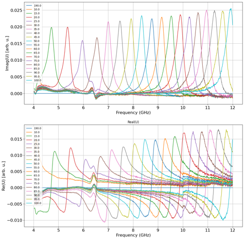
The Vector Network Analyser is typically used to characterize the electrical response of a system as a function of frequency (from 10 MHz up to 40 GHz). The tool can apply a calibrated electrical stimulus of specific frequency and measure the reflected/transmitted voltage and current both in magnitude and phase. The resulting measurement presents a detailed electrical characterization of the system in terms of equivalent impedance of the network or device under test (DUT) as a function of frequency throughout the measured frequency range. Obtaining this information as a function of frequency enables detailed electrical description of complex electrical response in a simple and concise way. The technique is extremely powerful in the sense that it can provide complete electrical response information on any linear electrical system. It is commonly used to measure high frequency devices as well as measure the material properties in extended frequency ranges. The VNA can be coupled with an external dipole/quadrupole electromagnet to perform broadband FMR and spin wave spectroscopy. FMR VNA is a powerful all electric experimental technique that can be used to resolve fundamental material properties (e.g. saturation magnetization, damping coefficient, gyromagnetic ratio). The FMR VNA can sweep the frequency of the input signal and measure reflected/transmitted signal while the external magnet can sweep the magnetic field providing much bigger set of data. The quadrupole magnet can generate a vectorial magnetic field tunable in the sample plane with a maximum intensity > 0.2 T (> 0.15 T in the dipolar configuration). The sample is excited by passing the RF signals through a standing coplanar waveguide (CPW) over which the sample is positioned. The VNA setup can be used to detect spin waves propagating in the magnetic ordering of a material under study. The VNA can be connected to a pair of parallel microwave antennas through RF microprobes (e.g. coplanar waveguides and ground-signal-ground (GSG) RF probes). Each microstrip is connected to a separate port of the VNA. Spin waves are excited from the first antenna (transmitter) and detected by the second one (receiver). This analysis is most useful to understand the behavior of magnetic materials.

Available instruments

Select instruments to view their specifications and compare them (3 max)

Lab's Facility

Milano

POLIMI-POLIFAB

Instruments' description and comparison

Also consider

A typical electron beam lithography tool is a vector-scan direct-write tool with a Gaussian shaped beam. The electrons are accelerated (typically 5 keV to 30 keV), depending on the application) and the beam scanning is controlled by special beam-deflection systems. The beam is directed to a position in the main deflection field, where a pattern is written by stepping around the electron beam.  For larger patterns, the pattern is divided into main field blocks, which are completely exposed one-by-one after mechanically moving the substrate to the right position. A laser interferometer can often measure the actual stage position, and this signal is fed back to the deflection system with a resolution even below a nanometer.

Electron-beam spot sizes can be focused to sub-10 nm in diameter. At the same time, a wide range of beam currents is available (depending on the tool, typically a few pA to 10 nA). This enables high-throughput as well as high-resolution exposures with a high degree of versatility. In addition, with high accelerating voltages, thick layers of e-beam resists can be exposed, with small forward electron scattering. With electron-beam lithography, aligning multiple levels of lithography with very high overlay precision is possible, with manual or automatic detection of alignment markers. Most systems can handle full wafers, mask blanks, and custom shaped samples and provide automatic laser focusing for height measurement. Users can implement or supply their designs in most standard formats, while specialized software is usually available for pattern preparation and proximity effect correction. Typical high resolution electron-beam resists are, among others, PMMA (positive tone) and HSQ (negative tone).

Read more

EBL

Electron Beam Lithography

Lithography & Patterning

The principle of wet etching processes is the conversion of a solid material into liquid compounds using chemical solutions. The selectivity is usually very high, and for most solutions is greater than 100:1. Material removal rate for wet etching is usually faster than the rates for many dry etching processes and can easily be changed by varying temperature and concentration of the active species. Multiple wafers can be etched simultaneously in batch etching; in this case filters and circulating pumps prevent particles from reaching the wafers.

When a material is attacked by a liquid or vapor etchant, it can be removed with isotropic (uniformly in all directions) or with anisotropic etching. In anisotropic etching the liquid etchants etch crystalline materials at different rates depending upon which crystal face is exposed to the etchant.

Wet or dry etching processes are common steps in the technological process flow for obtaining the material under study well patterned, isolated and ready to be contacted.

In particular, the process flow usually contains the required suite of pattern transfer and/or etching processes for ancillary materials, such as silicon nitride, silicon oxide, polysilicon that can be used as etching masks, implantation and diffusion barriers, dielectric barriers, spacers or conductive layers. Those materials can be etched and patterned by chemical wet etching or by Reactive Ion Etching (RIE) using appropriate masks or making use of lift-off process. Those materials can be used themselves as etching masks (for instance in the case of Al layers for deep RIE patterning of substrates), or as adhesion or barrier layers or directly as layers for providing the required electrical contact. 

Read more

WE

Wet Etching

Lithography & Patterning