Explore the offer
Growth & Synthesis / Physical depositions of thin films
Molecular Beam Epitaxy
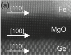
Molecular beam epitaxy (MBE) is a growth technique for the deposition of high quality and high purity epitaxial layers on suitable substrates. It is mainly used for the growth of semiconductors, oxides and chalcogenide materials with sub-nanometer control of the film thicknesses.
MBE systems are also used to make nanostructures, including quantum dots and nanowires, and epitaxially layered structures and heterostructures, for the fabrication of lasers, photodetectors, light-emitting diodes and other optoelectronic/photonic devices, as well as hybrid semiconductor-superconductor platforms.
Thermally produced atomic or molecular beams of the constituent materials migrate in Ultra High Vacuum (UHV) environment until impinge on a heated substrate where they are incorporated. The growth rate is generally very slow, of the order of one monolayer (ML) per second, allowing a ML control of the deposition.
The UHV environment allows for the use of diagnostic techniques during the growth as the reflection high energy electron diffraction (RHEED) and the integration of the growth system with UHV surface characterization techniques. In addition, optical pyrometry/reflectometry allows for precise closed-loop monitoring and control of multilayer thin film growth (substrate temperature, film thickness, and growth rate). When combined with the referred ability to perform in-situ high-resolution structural and electronic diagnostics of the films as they are being deposited, MBE provides the ideal scenario for understanding many of the fundamental structural and physical properties of ultrathin inorganic film systems.
Available instruments
Select instruments to view their specifications and compare them (3 max)
Lab's Facility
Trieste
CNR-IOM@TS
Trieste
CNR-IOM@TS
Trieste