Explore the offer

Growth & Synthesis / Chemical depositions of thin films

Chemical Vapour Deposition

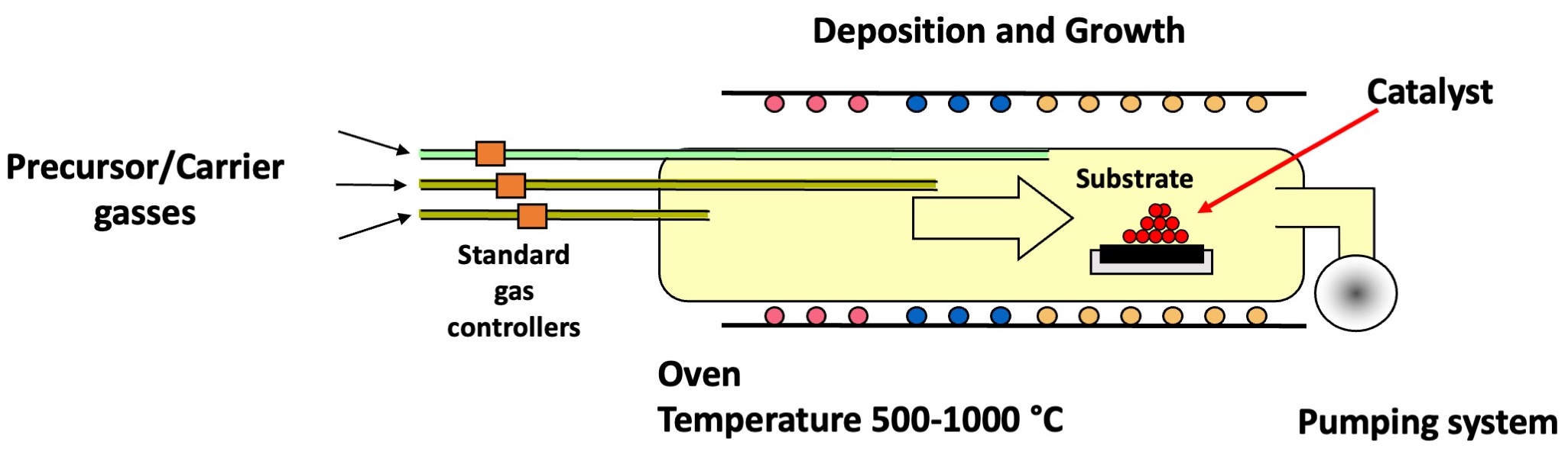
CVD is a thermal process because a certain thermal energy is needed to decompose the gas precursors and reassemble them in the material to be synthetize. Generally,  in a CVD process, the substrate is maintained at high temperature while it is exposed to the volatile precursor/s, usually carried by an inert carrier gas (like Ar). High temperatures are usually required to decompose the precursors and to reassemble the products in the growing material.The use of a catalyst may allow to decrease the process temperature and to select the location and the nanostructure of the growning film. Together with the carrier and precursor gasses, other gasses, like etching gasses (like H2, NH3, …), may be used to avoid the formation of undesired species and to enhance the synthesis of the desired material. In high pressure CVD (atmospherics pressure) the use of an inert carrier gas helps to avoid gas-phase reactions (homogenous deposition) and favor the synthesis trough surface processes (heterogeneous deposition). When CVD is done at low pressure, the process is called Low Pressure CVD (LPCVD). In this case the reactions in the gas-phase of the precursors are reduced and the higher diffusivity of the precursor species favor to decorate cavities and led to get homogeneous coatings when a topography is present. The homogeneity is also spurred by the process temperature, which favors the mobility of the atomic/radical species along the surface. Process pressures are usually in the millitorr-torr range and process temperatures range is 400-800C (depending on the energy needed to decompose the precursors). To favor the precursor gas decomposition and to lower the CVD temperature, the CVD process may be assisted by a plasma, and in this case the technique is referred as plasma-enhanced CVD (PECVD). This usually allows lowering the temperature of the process to a few hundred centigrade degrees, which can be run on less temperature resistant substrates or without setting off temperature triggered unwanted processes. 

The present implementation of the technique is suitable for mm to cm-size samples as those typically studied by spectroscopy and microscopy.

Available instruments

Select instruments to view their specifications and compare them (3 max)

Lab's Facility

Catania

CNR-IMM@CT

Bologna

CNR-ISMN@BO

Bologna

CNR-ISMN@BO

Bologna

CNR-ISMN@BO

Bologna

CNR-ISMN@BO

Bologna

CNR-ISMN@BO

Trento

CNR-IFN@TN

Catania

CNR-IMM@CT

Instruments' description and comparison

Also consider

Scanning Tunneling Microscopy (STM) allows imaging conductive surfaces at the atomic scale. It is possible to characterize the distribution of surface terraces and steps, as well as to determine the atomic arrangement of (ordered) surface (over)structures.

In STM, an atomically sharp tip is scanned on a surface at a few-angstrom distance, while a bias voltage is applied between these two electrodes, so that a current flows due to the quantum tunneling effect. The intensity of the tunneling current depends exponentially on the tip-surface distance and can therefore be used to reconstruct a morphologic image.

STM is a local technique: while high-resolution can be achieved on small (nanometer sized) areas, information on large-scale (micron sized or more) is lost, and measurements have to be repeated systematically on several regions of the sample to get statistically relevant information.

Due to stability performances, STM experiments are typically time-consuming. The technique is applicable both in air and in vacuum. Ultra-high-vacuum (UHV) is required for the characterization of delicate, atomically clean systems and for performing measurement at cryogenic temperature.

The STM signal is not purely topographic, but brings also information on the local density of electronic states. Scanning tunneling spectroscopy (STS) is an extension of STM that provides information about the density of electrons in a sample as a function of their energy. Inelastic tunneling spectroscopy (IETS) is a challenging extension for the investigation of vibrational states at liquid helium temperature. The STM tip can also be used to manipulate single atoms and molecules.

By acquiring sequences of consecutive images, STM can also be used to investigate at the atomic scale dynamical processes occurring on the surface of conductive samples, with a typical acquisition time of few tens of seconds per image. To further extend the range of accessible details in this kind of measurements, NFFA-Europe makes for the first time available to external users the access to a FastSTM option for high-speed imaging with a VT-STM microscope at CNR-IOM.  Thanks to this option, it is now possible to image with atomic resolution dynamical processes as chemical reactions, diffusion and growth, with a frame rate up to 100 images per second on regions few-nanometer wide.

Read more

STM

Scanning Tunneling Microscopy

Advanced Characterization and Fine Analysis