Explore the offer
Advanced Characterization and Fine Analysis / Electron, Ion and photon beam microscopy
Low Energy Electron Microscopy
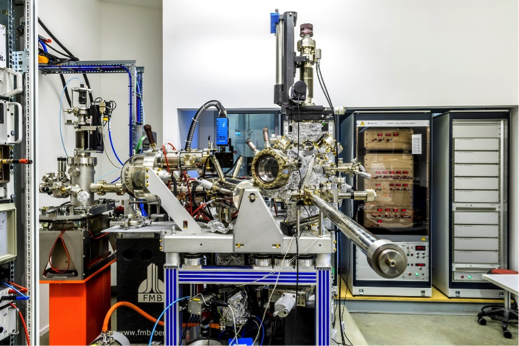
SPELEEM microscope uses low-energy electron as information carriers. Unlike scanning microscopy, electrons are collected simultaneously from an illuminated area of several tens of micrometers. The image formed by the magnification lenses can be acquired even in video-rate. SPELEEM is capable of combining microscopy, spectroscopy and diffraction to obtain a comprehensive characterization of conductive and semiconductive samples from the meso- to the nanoscale. Thanks to its versatility, SPELEEM can be employed to study model systems in the fields of nanotechnology, material science, catalysis, energy storage, organic and inorganic thin films, and low-dimensional materials.
SPELEEM is equipped with an hemispherical energy analyzer and two complemetary illumination sources - an electron gun and a UV lamp. Using the electron gun, the following operational modes are available.
- Low-Energy Electron Microscopy (LEEM): electrons hit the sample with a selected, low kinetic energy (typically 1-100 eV), are backscattered elastically from the surface and are collected by the optical elements to form a magnified image on a 2D electron detector. Electrons can be filtered in energy and acceptance angle while traveling through the optical path. Several contrast mechanisms (including dark-field imaging) allow the determination of the lateral dimensions of regions with a given crystal structure, the thickness distribution of thin overlayers with monolayer resolution, the imaging of monoatomic surface steps and other morphological features. The best resolution achievable in optimal conditions is 10 nm.
- Micron-sized Low-Energy Electron Diffraction (µLEED): by displaying the backfocal plane of the objective lens on the 2D electron detector, the microscope give access to a high-quality diffraction pattern of the backscattered electrons. The incident electron beam can be segmented to illuminate a sub-micron sized area, enabling the collection of a diffraction pattern from a single surface domain. The interacting kinetic energy of the electrons can be varied to obtain high-quality LEED-I(V) spectra.
Using UV sources, PEEM mode can be implemented in the same instrument.
SPELEEM experimental facility can accommodate conductive and semiconductive samples hosted by Elmitec and Flag-style sample holders. Heating stages are provided in the microscope chamber and in the preparation chamber. Other equipment available includes a gas line with precision leak valves, e-beam evaporator, preparation chamber with noble-gas sputtering, fast entry lock for sample loading.
Available instruments
Select instruments to view their specifications and compare them (3 max)
Lab's Facility
Trieste