Explore the offer

Advanced Characterization and Fine Analysis / Ultrafast-Spectroscopy

Ultrafast-Spectroscopy
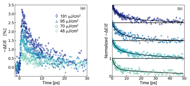
Ultrafast spectroscopy (or Pump-probe spectroscopy) is a technique used to study the dynamics of excited states in various materials, such as molecules, semiconductors, and solids.

It involves the use of two laser pulses. The first laser pulse, the "pump," excites the sample, elevating electrons from the ground state to an excited state. This initiation creates a non-equilibrium condition in the sample. After a controlled delay, a second laser pulse, the "probe," is sent through the sample. The probe pulse interrogates the sample to gather information about the transient states and the evolution of the excited states over time.

By varying the delay time between the pump and probe pulses, researchers can create a time-resolved picture of the dynamic processes occurring in the material. This time resolution can be on the order of femtoseconds (10^-15 seconds), allowing scientists to observe ultrafast phenomena.

These techniques provide insights into ultrafast processes, such as electronic transitions, high-order harmonics generation, molecular vibrations, and energy transfer mechanisms, that occur on very short time scales. It helps in understanding the fundamental properties of materials, such as the relaxation times of excited states, carrier dynamics in semiconductors, topological effects and the mechanisms of photochemical reactions.

Other possible studies can cover the world of solar cells, light-emitting devices, and photocatalysts, where understanding the dynamics of excited states is essential for improving efficiency and performance. Moreover, in biophysics and biochemistry, pump-probe spectroscopy can be used to investigate the dynamics of biomolecules, such as the folding and unfolding of proteins, photosynthesis mechanisms, and the behavior of molecular motors.

Available instruments

Select instruments to view their specifications and compare them (3 max)

Lab's Facility

Trieste

CNR-IOM@TS

Milano

CNR-IFN@MI

Milano

CNR-IFN@MI

Milano

CNR-IFN@MI

Trieste

CNR-IOM@TS

Trieste

CNR-IOM@TS

Roma

CNR-ISM@RM

Instruments' description and comparison

Also consider

Transmission Electron Microscopes (TEM) and Scanning Transmission Electron Microscopes (STEM)  are designed for high-resolution imaging and analysis.
In both cases, high energy electrons, incident on ultra-thin samples called TEM lamella (typically <100nm), travel through the specimen.
Depending on the density, crystallinity, orientation, etc. of the material present, electrons are scattered differently, giving rise to an image of the sample with different contrast features according to specimen properties and to the microscope setup.
Usually, the magnified image of the sample is focused on a CCD or CMOS camera. On the same system is also possible to acquire the electron diffraction produced by a specific area of the sample.

Modern TEM are equipped with a Cold Field Emission Gun (FEG) or with a Schottky FEG, making them suitable for materials science, nanotechnology, and various fields requiring detailed structural and compositional analysis in a local nanoscale. Indeed, point resolution below 0.3 nm at 200kV in TEM mode can be reached, according to the
instrument configuration.


In the STEM mode, electrons pass through the specimen, but, the electron optics focus the beam into a narrow spot which is scanned over the sample in a raster. The rastering of the beam across the sample makes these microscopes suitable for analysis techniques.


According to the specific configuration (see details and the specific availability below, referred to each instrument and facility), the microscope can be equipped with a selection of multiple detectors enabling different techniques, such as Energy-Dispersive x-ray Spectroscopy analysis (EDS), electron energy loss spectroscopy (EELS), STEM detectors in bright field (BF), annular bright field (ABF), annular dark field (ADF) for diffraction contrast, high-angle annular dark field (HAADF) for Z-contrast.


EELS/EDS system control software enables point-by-point signal acquisitions, for the analysis of spectra and maps.
Sample preparation (see details and the specific availability below, referred to each instrument and facility) is a crucial part in TEM experiments.

High quality TEM specimens have a thickness that is comparable to the mean free path of the electrons that travel through the samples, which may be only a few tens of nanometres. Preparation of TEM specimens is specific to the material under analysis and the desired information to obtain from the specimen. Sample preparation laboratories are equipped with the basic tools (diamond saw, polisher, dimpler, ultrasonic cutter, precision ion polishing system, plasma cleaner) commonly used in conventional thinning procedures.

Read more

TEM/STEM

Transmission Electron Microscopes and Scanning Transmission Electron Microscopes

Advanced Characterization and Fine Analysis

Spectroscopic Ellipsometry (SE) is a contact-free, nondestructive method for the characterization of the dielectric and optical properties (refractive index, absorption coefficient, anisotropy) and structural properties (roughness, thickness and intermix of layers) in the thickness range of < 1 nm to few µm.

Ellipsometry is an accurate technique for calculating materials’ parameters, including complex refractive index or dielectric function. The samples are measured in reflection and the information is given based on the change of the polarization of the reflected light. Standard SE methods measure the Fresnel reflection coefficients as a function of wavelength only. While variable angle SE (VASE) measures the sample’s coefficients in s- and p-polarized light as a function of wavelength and angle of incidence. In addition, thanks to the vertical configuration it can be measured also the sample transmittance to be coupled with the ellipsometric data during fitting. All measurements can be done with a motor stage on a 4x4cm area.

Depending on the spectral coverage of a VASE instrument, dielectrics, semiconductors, and metals can be characterized. Typical applications are the characterization of manufactured thin films used in devices. Sample size can vary from 1x1cm up to a 6” wafer.

Finally, the measurements, thanks to a closed cell, can be performed in an N2 environment in the case of air-sensitive samples and or by varying the temperature in the range -90°C up to 600°C to identify phase changes.

Read more

Ellipsometry

Ellipsometry

Upscale to Intermediate TRL