Explore the offer
Growth & Synthesis / Physical depositions of thin films
PVD sputtering

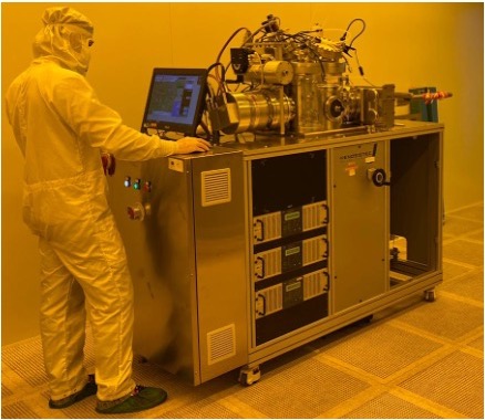
Physical vapor deposition (PVD) by sputtering is a powerful technology for creating thin films with varied compositions, structures, and properties. This process allows the uniform application of very different materials (metals, alloys, oxides, and nitrides) on a broad range of substrates, ranging from semiconductor wafers to architectural glass, and enables deposition of films for applications that impose stringent requirements on the high morphological quality and composition of surfaces, e.g., roughness, grain size, or stoichiometry. To deposit such high-quality films, PVD Sputtering systems are typically optimized for relatively low deposition rates, which enable reproducible deposition of films down to nm-range thickness. Conformal coverages are also easily achieved by sputtering with respect to evaporation.
Thin deposition by sputtering has been used for over a century: magnetron sputtering (DC and RF) is used to boost the deposition rate and reactive sputtering is used to deposit oxides/nitrides from a metallic source.
In a sputtering chamber working under high vacuum conditions, deposition rate and film characteristics can be tuned by the power loading over the target, the gas flow rate and partial pressure management.
Additional capabilities in PVD Sputtering systems can include substrate heating, application of a magnetic field, mechanical movement to produce wedge layers, or automated systems for handling wafers.
Sputtered thin-film materials have demonstrated applicability across various sectors, such as in electronics, semiconductor devices, transparent thin-film transistors, photoelectric detectors, optical coatings, solar cells, aerospace, biomedical domains.
The wide use of the PVD Sputtering tools in the industry also makes this approach beneficial for projects that aim at the eventual technology transfer to industrial partners.

Available instruments
Select instruments to view their specifications and compare them (3 max)
Lab's Facility
Catania
CNR-IMM@CT
Bologna
CNR-ISMN@BO
Bologna