Explore the offer
Upscale to Intermediate TRL / Back-End
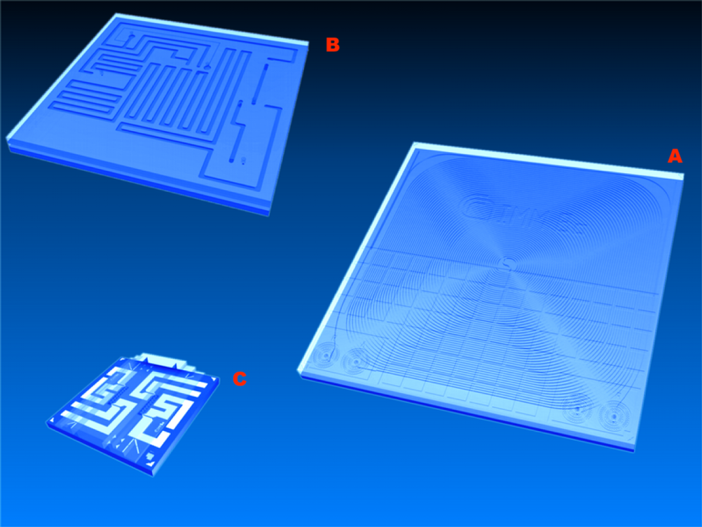
Wafer Bonder
Wafer bonding is a technology to combine two substrates in order to achieve a mechanically stable connection between them. Bonding could be performed between two silicon wafers, but can also be employed for various substrates, including glass wafers or non-silicon semiconductor (e.g., GaAs) wafers. This technology is applied for the fabrication of MEMS/MOEMS devices, for stacking devices in 3D integration, or for wafer-level packaging.
The wafer bonding processes can be subdivided into direct bonding techniques, such as fusion and anodic bonding, and processes requiring an intermediate layer, a metal, dielectric, or adhesive film, for bond formation, such as solder and eutectic bonding, or glass-frit bonding. In most cases, flat, smooth and clean surfaces are needed for good bonding results.
Fusion bonding is based on the fact that two mirror-flat, clean wafer surfaces will adhere to each other even at room temperature if brought into contact. The process is executed at room-temperature, and bonding is attributed to attractive van der Waals forces.
Anodic bonding is the most widely used wafer bonding technique in the microsystems area. In anodic bonding, a silicon wafer is usually bonded to a sodium-rich glass wafer by applying voltages in the range 200–1500 V between the two wafers at temperatures in the range of 300–450 °C. Anodic bonding can be also used to bond two silicon wafers with a sputtered or evaporated glass film in between.
In solder or eutectic bonding a suitable solder material is deposited in the bond area between a substrate wafer with microsystem components and the capping wafer. The two wafers are aligned to each other and brought into contact and the temperature is increased until the solder reflows and creates a bond between the wafers. The solders can be applied by screen or stencil printing, electroplating, or using solder preforms.
Glass-frit bonding is based on a low melting glass paste, printed by screen printing and melted at temperatures around 430 °C under pressure during the bond process. Glass frit bonding is mainly used to join two silicon wafers, but can be applied to a wide range of surface materials commonly used in microsystems technology, including silicon dioxide, silicon nitride, or aluminum.
Available instruments
Select instruments to view their specifications and compare them (3 max)
Lab's Facility
Bologna